Semiconductor products were more affected than any other by COVID-induced supply-chain issues felt around the world. International political tensions have only prolonged and exacerbated the problem.
By Lisa Eitel | Executive editor
Every modern gadget, vehicle, smart device, and appliance is peppered over with semiconductors galore — offering that singular function of processing power that is the defining characteristic of advanced electronic products most valued today. The issue laid bare by COVID is how the cosmopolitan yet non-diversified nature of the semiconductor industry currently renders it vulnerable to disparate issues across the globe.
ABB Robotics worked with Easy Field Corporation (EFC) to design a semiconductor unpacker employing cleanroom IRB 1200 robots to connect stations and IRB 4600s to boost capacity. A barcode scanner confirms label information; then an IRB 4600 robot transfers one front opening shipping box (FOSB) to a station for nitrogen filling.
In many cases, a small handful of companies execute chip processing in Europe; chip-processing machine building in California and Japan; chip testing in Southeast Asia; and assembly into the final product (where applicable) in China. Of intensified concern now is how more than half of all semiconductors and more than 90% of all advanced semiconductors are made in the tiny island nation of Taiwan. Fabrication plants (fabs or foundries) there including Taiwan Semiconductor Manufacturing Co. (TSM) supply more than half of all the world’s semiconductors and nearly all advanced semiconductor chips (featuring extremely miniaturized features). However, the looming possibility of China’s claim of Taiwan as a province could threaten this industry.
An ABB IRB 1200 uses an ultrasonic cutter (that doesn’t generate dust) to slice the aluminum bag containing the FOSB. Then the cleanroom robot passes the box being processed to another IRB 1200 station. Because a robotic arm passes semiconductor-manufacturing waste to a centralized station, loading and unloading goes faster. Image: ABB
Heightening tensions include Trump-era sanctions restricting Chinese telecommunications and electronics giant Huawei from employing U.S. software or technology and Biden-era sanctions as well as the 2022 Creating Helpful Incentives to Produce Semiconductors (CHIPS) and Science Act. The latter designates $280B for coordinated spending over the next decade on U.S. including semiconductor R&D and commercialization ($200B); manufacturing and workforce development ($52.7B); and chip production tax credits ($24B). The act is similar to the CHIPS Act officially adopted by the European Council of the European Union in December 2022. Read on to get Design World panelists’ views on these initiatives.
Meet the experts
Justin Lackey | Product manager — systems • Bosch Rexroth
Kelly Walden | V.P. of manufacturing • Bishop-Wisecarver Corp.
Jonathan Schroeder | Executive V.P. • PBC Linear
Pamela Kan | President and owner • Bishop-Wisecarver Corp.
Richard Johannes | Director of engineering and innovation • LEMO USA
Steven Lassen | Product & applications manager • LEMO USA
Tom Schroeder | Executive V.P. • PBC Linear
Andy Zaske | V.P. of sales and marketing • Tolomatic
Boaz Eidelberg | CTO • SAAR Inc.
Nathan Andaya| Director — Techline strategic business unit • LINAK U.S.
Camilo Orjuela | Industry segment manager – semiconductor and solar • Bosch Rexroth Corp.
Chris Gumas | Director of marketing • Ruland Manufacturing
Mike Beasley | U.S. semiconductor production • maxon
Andrew Jung | Director of engineering • Bishop-Wisecarver
Chris Gottlieb | Director — Drives and controls • Kollmorgen
What are your views on government incentives to increase U.S. competitiveness in semiconductor manufacture?
Lackey: Although the semiconductor market is starting flat for 2023, we’re projecting a significant increase in coming months and heading into 2024 — especially as government incentives have bolstered U.S. demand forecasts. That said, we still maintain a presence in the Asia Pacific region as a global supplier of semiconductor tool products.
Walden: I support most initiatives by our government that encourage investment in manufacturing while also giving the U.S. a strategic and defensive advantage in the global economy.
Orjuela: The increasing complexity of semiconductor designs, along with rapidly increasing demand for semiconductors from every market segment, is significantly challenging fab operators and tool builders to create more advanced production while still keeping costs under control. With skyrocketing costs — building a semiconductor fabrication facility alone is estimated to cost between $15B to $20B — chip manufacturers face a dilemma: Should they buy more tools and expand plants or find ways to improve throughput using more adaptable and efficient automation technologies?
Eidelberg: Most fabs operate in Taiwan, Japan, China, the U.S., and Germany and have been in business for decades. The challenge is that fabrication centers cost billions of dollars to build and run, and they require highly skilled employees to operate. What’s more, key semiconductor-manufacturing processes (including lithography) employ extreme-precision machines needing protection from disturbances due to seismic activity, airport noise, passing trains, highway traffic, and local handling equipment.
To compete with existing overseas fabrication facilities, I believe U.S. funding should sponsor universities and semiconductor-equipment manufacturers primed for innovative product development using AI/ML technology. Ultimately, this would allow manufacturing processes to make autonomous realtime decisions in response to uncertain manufacturing environments. IoT, 5G, cloud, and possibly cryptocurrency systems could complement such autonomous operations for better time to market, reliability, quality, productivity, and cost.
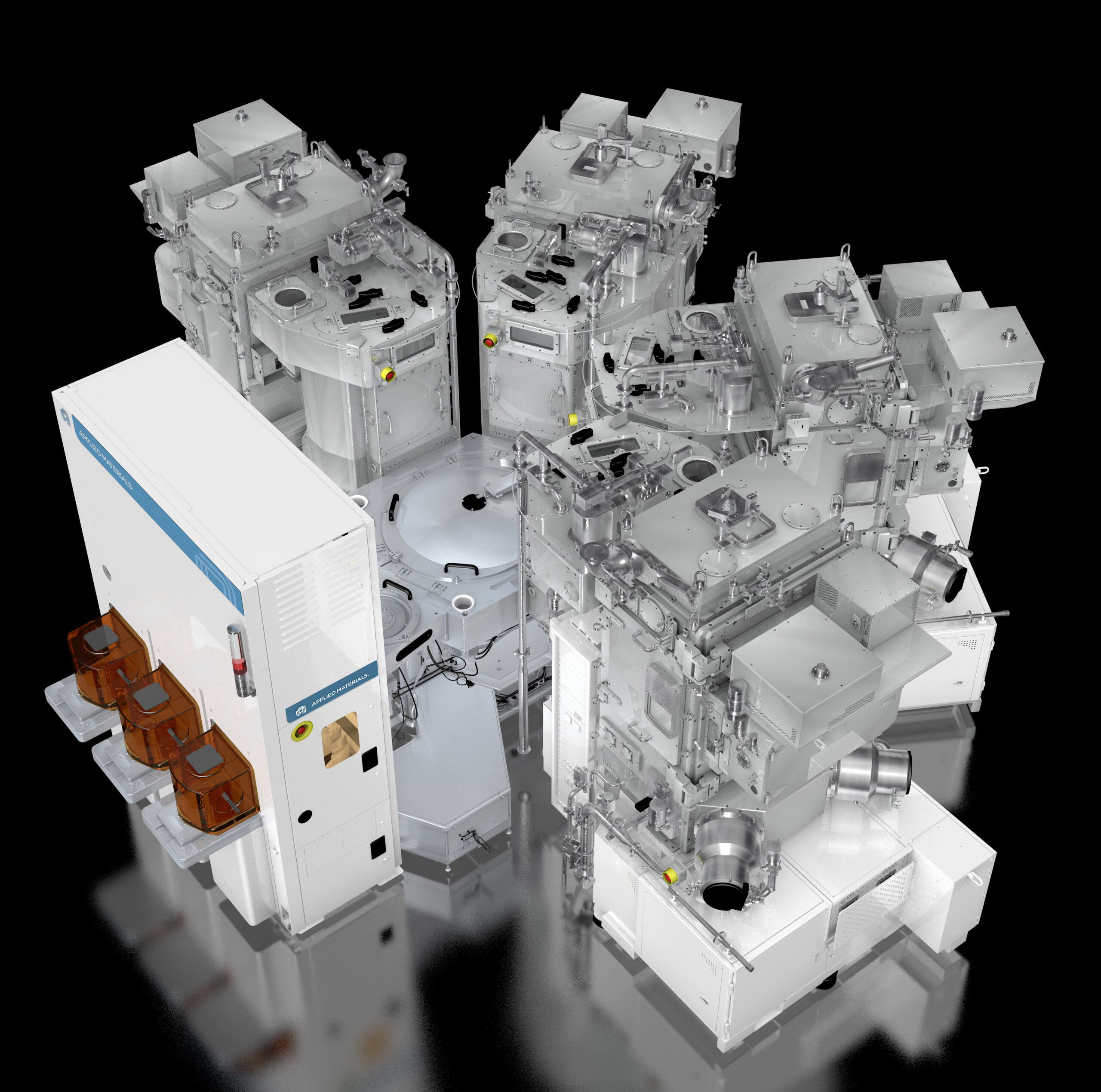
Applied Materials’ new Centura Sculpta patterning technology lets chipmakers create high-performance transistors and interconnect wiring with a single manipulatable extreme ultraviolet lithography (EUV) pattern. In short, the technology aims to achieve the fine-featured results of double patterning but at a lower cost, complexity, and environmental impact. This is just one example of recent developments in semiconductor manufacture. Image: Applied Materials
Gumas: Ruland products are used by most of the world’s largest semiconductor equipment manufacturers. New equipment design for American and European companies is primarily done in those markets with final production usually taking place in China. If some of the manufacturing moves to the U.S., there’s no direct advantage for us. The equipment that may soon be made in the U.S. is already using high-end components from manufacturers such as Ruland.
That said, as a domestic manufacturer, we’re happy to see the U.S. investing in any part of the manufacturing sector. It’s likely to stimulate growth in the various trades required to support the industry that both industry and government have underfunded over the past 30 years.
T. Schroeder: The government has made a positive step investing in domestic semiconductor manufacturing and development. Billions of dollars will flood into the U.S. marketplace to build and equip these factories. One caveat is it will take years before these factories are producing at volume. What’s more, the Biden administration’s simultaneous imposition of semiconductor export limits to China has left a supply for which the U.S. semiconductor marketplace doesn’t have demand to replace.
Kan: While I’m happy to see this development, I still feel it’s a bit myopic. The CHIPS and Science Act is a good first step, but the government should’ve learned from the COVID experience that many critical areas of the supply chain are no longer viable in the U.S. A more holistic approach must be adopted to increase the growth and innovation of the U.S. industrial market.
Andaya: Onshoring semiconductor manufacturing to the U.S. will reduce the risks associated with having a manufacturing partner in China. The biggest caveats are the ramifications regarding price.
Gottlieb: Kollmorgen both uses semiconductors and sells into the semiconductor servo motion-control market. Quality, ease of programming, and optimized power as well as motion output are all key in this market. Diversification in physical locations for semiconductor manufacturing is beneficial to the entire motion-control industry to help improve the supply consistency of industrial semiconductors used in our products.
More on the CHIPS and Science Act
Signed into law in Q3 2022, CHIPS has already spurred semiconductor research and manufacturing initiatives. If all goes well, two Arizona TSM fabs are expected to begin production of 4-nm chips next year (including for Apple) with advanced 3-nm chip production to follow in two years. As mentioned, the processes are maximally complex. Chip blueprints designed in oft-proprietary software might come from halfway across the globe to be executed on specialized silicon wafers using engineered gasses.
How are your components and systems used in the equipment specialized for semiconductor production?
Kan: In the chipmaking process, our specialized linear bearings are used for shuttling products into high-temperature areas.
T. Schroeder: We provide precision ground bright bar and support rails for linear motion in silicon-wafer manufacturing equipment.
Zaske: We fully support the onshoring of semiconductor manufacturing. Tolomatic products are used in the wafer growth process where reliability, stability, and precision can make a significant difference in yields and quality. Our Minnesota manufacturing location makes for fast leadtimes, product modifications for specific applications, and quick accessible support for North American design engineers.
Lackey: Manufacturing the components that go into larger systems and subassemblies has helped us grow our footprint in semiconductor tool manufacture. We’re currently supplying linear ball rail systems and ballscrew drive systems for various semiconductor manufacturing processes. These include wafer-manufacturing and lift systems, wafer tool-transfer systems, wet benches, material-deposition equipment, and etching and chemical-process machinery. Our linear guidance and drive technologies also go into standard catalog products and linear modules.
The type of linear modules we’re supplying for semiconductor tools are mostly ballscrew-driven modules such as our PSK precision modules with integrated linear guidance and compact modules (CKK) with dual ball rail guidance. Some smaller-volume projects employ our CKR compact belt drive modules with dual rail guidance. For these designs, compactness and accuracy aren’t as critical to the application.
Beyond our standard catalog products, we partner with design engineers to provide them custom subassemblies engineered to specification. These integrate our standard ball rail systems, ballscrew drives, and (in new tool designs) our rotary and linear motors.
Image: Dreamstime • Kittipong Jirasukhanont
Walden: Bishop-Wisecarver’s products are found in a broad range of wafer-fab and semiconductor-manufacturing equipment thanks to the smooth operation and the high quality of our products.
Jung: Our components are well suited to address the increasing demands on the semiconductor industry where clean environments are required. Continuous operation of equipment, including for wafer fabrication, is critical. That’s because failure during any semiconductor-making process can lead to expensive losses.
Complexity in semiconductor manufacture
Extreme-precision motion equipment cuts, etches, and deposits semiconductor details into silicon wafers and then transports finished chips onward.
What are some special challenges presented by semiconductor manufacture?
Orjuela: With the complexity of today’s chip processes, wafer transport must be rigorously controlled to be as stable and vibration-free as possible. Otherwise, vibration can generate particles that can contaminate the wafer or risk causing minute flaws in the wafer’s shape. At the same time, if the wafer transport is too slow, productivity suffers, and costs go up. We’ve developed deep expertise in solving the motion-control challenges for many front-end wafer handling applications. Our cross-technology portfolio combines open app-based controllers, compact servodrives specifically developed for semiconductor tool applications, and linear technology systems engineered to provide vibration-free accurate motion.
Using this portfolio, we create custom mechatronics assemblies incorporating technologies to address demanding semiconductor-making motion control, efficiency, and throughput requirements. These pre-engineered and tested assemblies help tool builders complete and deliver systems to chip manufacturers faster — and can help fab operators streamline processes and achieve smooth, precise motion and nanoscale positioning.

Bosch Rexroth addresses motion-control challenges for many front-end wafer handling applications.
Johannes: LEMO has several interconnect products used in networking, controlling, and video systems necessary for semiconductor fabrication equipment. These products provide hermetically sealed connections for bridging different segments of the equipment while maintaining essential environmental isolation. The connection applications include vapor deposition, ion implantation, etching, and chemical-mechanical polishing (CMP).
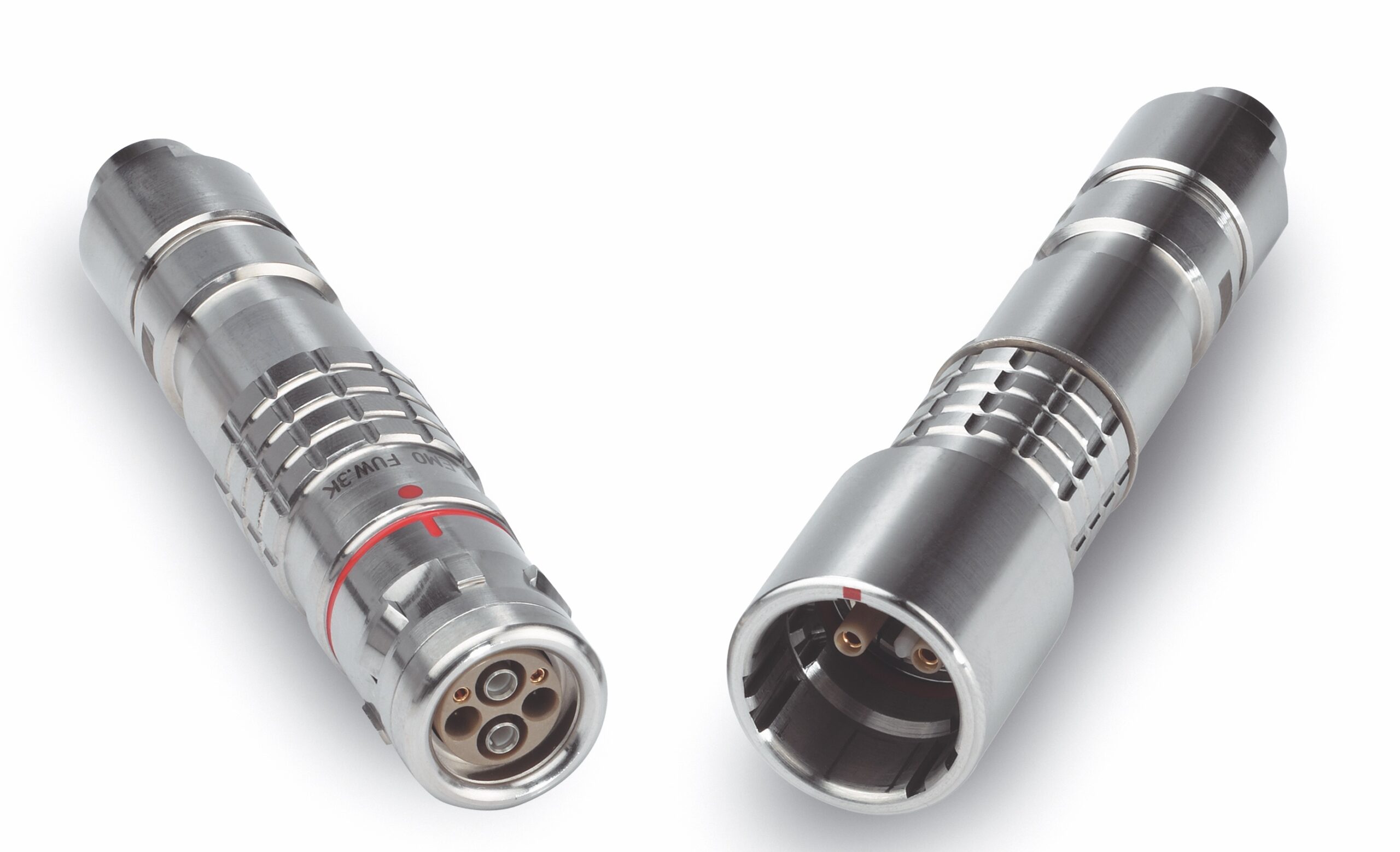
LEMO’s hybrid configuration integrates single-mode fiber, high voltage, and low-voltage elements within the same rugged housing.
Lassen: Many sensors and connectors on semiconductor-fabrication equipment operate in a cleanroom environment. In some cases, these components’ connectors must be assembled to the cable within the cleanroom … and that makes soldering a challenge. To avoid this issue, the use of crimp contacts eliminates any solder fumes from air contamination.
In semiconductor applications, heater power and temperature measurements can also be transmitted via our rugged and compact connectors. The connectors are easy to quickly connect and disconnect. In addition, they can accommodate type K or J thermocouple contacts — along with signal or power or even fiber optics within the same compact rugged connector housing.
Unfortunately in some high-vacuum settings of semiconductor manufacture, a condition called cold welding can occur. This is when mated halves of a connector set made from the same metal material are exposed to a vacuum and (over time) the two halves become welded together where the internal components touch. Cold welding can make it difficult or impossible to uncouple. To solve this problem, LEMO offers connectors with halves of different metals.
Beasley: We offer cost-effective solutions for the most demanding motion-control applications in the semiconductor market. maxon collaborates with industry leaders and leverages motion and application knowledge to provide precise systems employing compact rotational and linear brushless dc servodrives as well as controls. At the heart of semiconductor production is the expensive and delicate wafer itself. The wafer is rapidly moved through multiple automated processes — including lifting, positioning, holding, etching, polishing, and inspection from raw material to circuit chip end product — for maximal throughput and accuracy within tight size constraints.
Read other articles in the Design World Trends series at designworldonline.com/trends.
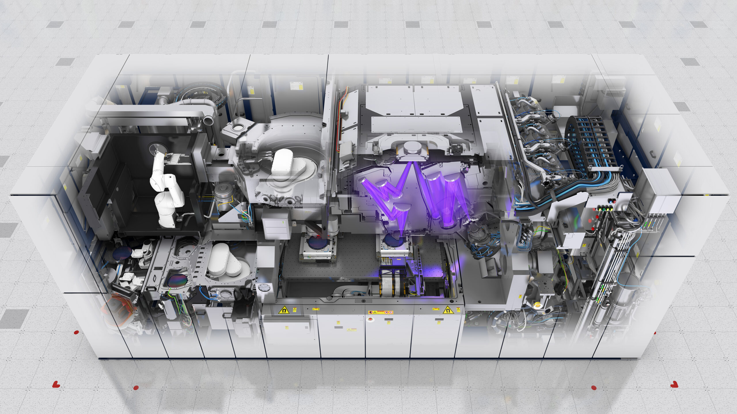
The ASML TWINSCAN NXE:3400B supports extreme ultraviolet-based lithography to impart 7 and 5-nm features on semiconductor products with high throughput and resolution to complement ASML’s argon fluoride immersion (ArFi) technology. Image: ASML
You may also like:
Filed Under: Semiconductor manufacture, Trends


